- 您现在的位置:买卖IC网 > Sheet目录510 > SI4561DY-T1-E3 (Vishay Siliconix)MOSFET N/P-CH 40V 8-SOIC
�� �
�
�Si4561DY�
�Vishay� Siliconix�
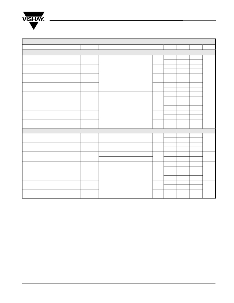
�SPECIFICATIONS� T� J� =� 25� °C,� unless� otherwise� noted�
�Parameter�
�Symbol�
�Test� Conditions�
�Min.�
�Typ.� a�
�Max.�
�Unit�
�Dynamic�
�a�
�Turn-On� Delay� Time�
�Rise� Time�
�Turn-Off� Delay� Time�
�t� d(on)�
�t� r�
�t� d(off)�
�N-Channel�
�V� DD� =� 20� V,� R� L� =� 4� Ω�
�I� D� ?� 5� A,� V� GEN� =� 10� V,� R� g� =� 1� Ω�
�P-Channel�
�V� DD� =� -� 20� V,� R� L� =� 4� Ω�
�N-Ch�
�P-Ch�
�N-Ch�
�P-Ch�
�N-Ch�
�P-Ch�
�7�
�11�
�10�
�15�
�15�
�36�
�14�
�20�
�20�
�30�
�30�
�60�
�Fall� Time�
�Turn-On� Delay� Time�
�Rise� Time�
�Turn-Off� Delay� Time�
�Fall� Time�
�t� f�
�t� d(on)�
�t� r�
�t� d(off)�
�t� f�
�I� D� ?� -� 5� A,� V� GEN� =� -� 10� V,� R� g� =� 1� Ω�
�N-Channel�
�V� DD� =� 20� V,� R� L� =� 4� Ω�
�I� D� ?� 5� A,� V� GEN� =� 4.5� V,� R� g� =� 1� Ω�
�P-Channel�
�V� DD� =� -� 20� V,� R� L� =� 4� Ω�
�I� D� ?� -� 5� A,� V� GEN� =� -� 4.5� V,� R� g� =� 16� Ω�
�N-Ch�
�P-Ch�
�N-Ch�
�P-Ch�
�N-Ch�
�P-Ch�
�N-Ch�
�P-Ch�
�N-Ch�
�P-Ch�
�9�
�9�
�16�
�49�
�17�
�79�
�16�
�35�
�10�
�14�
�18�
�18�
�30�
�80�
�30�
�120�
�30�
�60�
�20�
�25�
�ns�
�Drain-Source� Body� Diode� Characteristics�
�Continuous� Source-Drain� Diode� Current�
�Pulse� Diode� Forward� Current� a�
�I� S�
�I� SM�
�T� C� =� 25� °C�
�N-Ch�
�P-Ch�
�N-Ch�
�P-Ch�
�2.5�
�-� 2.5�
�20�
�-� 20�
�A�
�Body� Diode� Voltage�
�Body� Diode� Reverse� Recovery� Time�
�Body� Diode� Reverse� Recovery� Charge�
�Reverse� Recovery� Fall� Time�
�Reverse� Recovery� Rise� Time�
�V� SD�
�t� rr�
�Q� rr�
�t� a�
�t� b�
�I� S� =� 1.6� A�
�I� S� =� -� 1.6� A�
�N-Channel�
�I� F� =� 2� A,� dI/dt� =� 100� A/μs,� T� J� =� 25� °C�
�P-Channel�
�I� F� =� -� 2� A,� dI/dt� =� -� 100� A/μs,� T� J� =� 25� °C�
�N-Ch�
�P-Ch�
�N-Ch�
�P-Ch�
�N-Ch�
�P-Ch�
�N-Ch�
�P-Ch�
�N-Ch�
�P-Ch�
�0.78�
�-� 0.74�
�19�
�22�
�14�
�22�
�13�
�15�
�6�
�7�
�1.2�
�-� 1.2�
�30�
�40�
�25�
�35�
�V�
�ns�
�nC�
�ns�
�Notes:�
�a.� Guaranteed� by� design,� not� subject� to� production� testing.�
�b.� Pulse� test;� pulse� width� ≤� 300� μs,� duty� cycle� ≤� 2� %.�
�Stresses� beyond� those� listed� under� “Absolute� Maximum� Ratings”� may� cause� permanent� damage� to� the� device.� These� are� stress� ratings� only,� and� functional� operation�
�of� the� device� at� these� or� any� other� conditions� beyond� those� indicated� in� the� operational� sections� of� the� specifications� is� not� implied.� Exposure� to� absolute� maximum�
�rating� conditions� for� extended� periods� may� affect� device� reliability.�
�Document� Number:� 69730�
�S09-0220-Rev.� C,� 09-Feb-09�
�www.vishay.com�
�3�
�发布紧急采购,3分钟左右您将得到回复。
相关PDF资料
SI4562DY-T1-GE3
MOSFET N/P-CH 20V 8-SOIC
SI4563DY-T1-GE3
MOSFET N/P-CH 40V 8-SOIC
SI4565ADY-T1-GE3
MOSFET N/P-CH 40V 8-SOIC
SI4567DY-T1-GE3
MOSFET N/P-CH 40V 8-SOIC
SI4622DY-T1-E3
MOSFET N-CH D-S 30V 8-SOIC
SI4632DY-T1-GE3
MOSFET N-CH 25V 8-SOIC
SI4634DY-T1-E3
MOSFET N-CH D-S 30V 8-SOIC
SI4636DY-T1-E3
MOSFET N-CH/SCHOTTKY 30V 8SOIC
相关代理商/技术参数
SI4561DY-T1-GE3
功能描述:MOSFET N/P-Ch MOSFET 40V 35/35mohm @ 10V RoHS:否 制造商:STMicroelectronics 晶体管极性:N-Channel 汲极/源极击穿电压:650 V 闸/源击穿电压:25 V 漏极连续电流:130 A 电阻汲极/源极 RDS(导通):0.014 Ohms 配置:Single 最大工作温度: 安装风格:Through Hole 封装 / 箱体:Max247 封装:Tube
SI4562DY
功能描述:MOSFET 20V 7.1/6.2A 2W RoHS:否 制造商:STMicroelectronics 晶体管极性:N-Channel 汲极/源极击穿电压:650 V 闸/源击穿电压:25 V 漏极连续电流:130 A 电阻汲极/源极 RDS(导通):0.014 Ohms 配置:Single 最大工作温度: 安装风格:Through Hole 封装 / 箱体:Max247 封装:Tube
SI4562DY
制造商:Vishay Siliconix 功能描述:MOSFET DUAL NP SO-8
SI4562DY_06
制造商:VISHAY 制造商全称:Vishay Siliconix 功能描述:N- and P-Channel 2.5-V (G-S) MOSFET
SI4562DY-E3
功能描述:MOSFET 20V 7.1/6.2A 2W RoHS:否 制造商:STMicroelectronics 晶体管极性:N-Channel 汲极/源极击穿电压:650 V 闸/源击穿电压:25 V 漏极连续电流:130 A 电阻汲极/源极 RDS(导通):0.014 Ohms 配置:Single 最大工作温度: 安装风格:Through Hole 封装 / 箱体:Max247 封装:Tube
SI4562DY-T1
功能描述:MOSFET 20V 7.1/6.2A 2W RoHS:否 制造商:STMicroelectronics 晶体管极性:N-Channel 汲极/源极击穿电压:650 V 闸/源击穿电压:25 V 漏极连续电流:130 A 电阻汲极/源极 RDS(导通):0.014 Ohms 配置:Single 最大工作温度: 安装风格:Through Hole 封装 / 箱体:Max247 封装:Tube
SI4562DY-T1-E3
功能描述:MOSFET 20V 7.1/6.2A 2W RoHS:否 制造商:STMicroelectronics 晶体管极性:N-Channel 汲极/源极击穿电压:650 V 闸/源击穿电压:25 V 漏极连续电流:130 A 电阻汲极/源极 RDS(导通):0.014 Ohms 配置:Single 最大工作温度: 安装风格:Through Hole 封装 / 箱体:Max247 封装:Tube
SI4562DY-T1-GE3
功能描述:MOSFET 20V 7.1/6.2A 2.0W 25/33mohm @ 4.5V RoHS:否 制造商:STMicroelectronics 晶体管极性:N-Channel 汲极/源极击穿电压:650 V 闸/源击穿电压:25 V 漏极连续电流:130 A 电阻汲极/源极 RDS(导通):0.014 Ohms 配置:Single 最大工作温度: 安装风格:Through Hole 封装 / 箱体:Max247 封装:Tube